
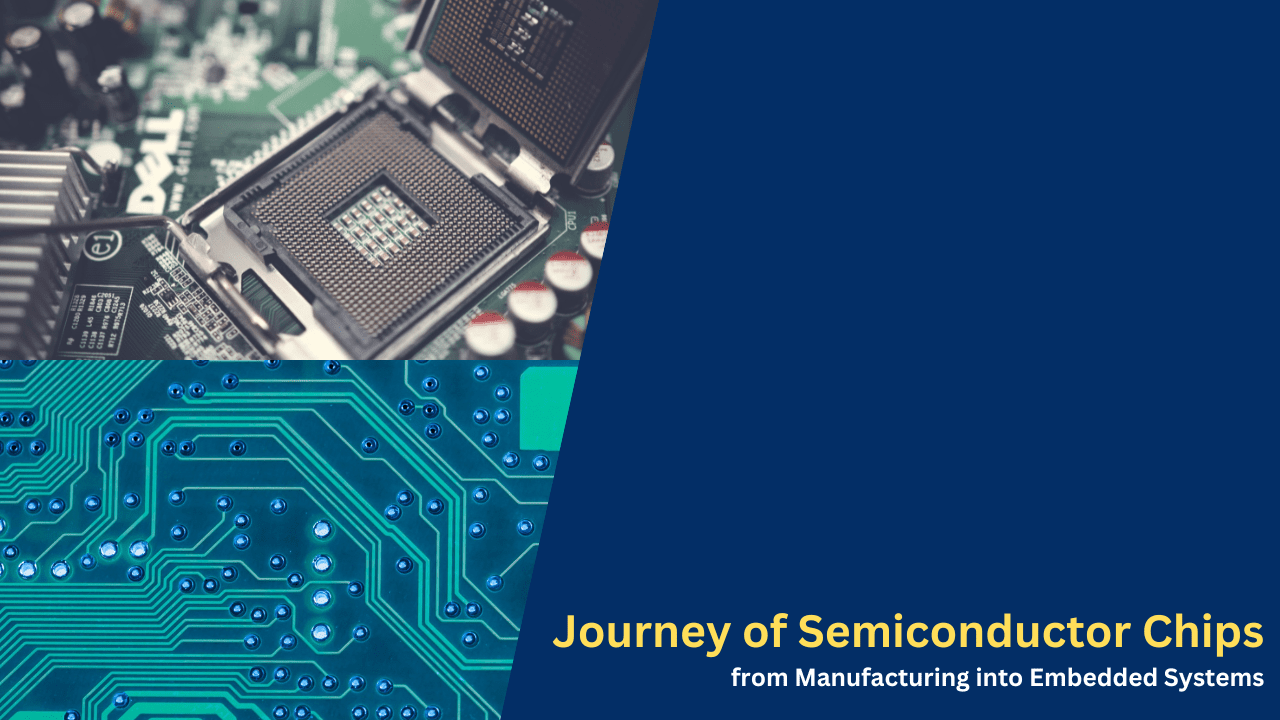
Journey of Semiconductor Chips from Manufacturing into Embedded Systems
Hello guys, welcome back to our blog. Here in this article, we will discuss the journey of semiconductor chips from manufacturing into embedded systems and briefly explain each stage.
Ask questions if you have any electrical, electronics, or computer science doubts. You can also catch me on Instagram – CS Electrical & Electronics.
- What Is Over The Air Updates, Features, Types
- Top Free Automotive Courses By Vector
- Types Of Cyber Attacks In The Automotive Industry
Semiconductor Chips from Manufacturing into Embedded Systems
A semiconductor chip’s journey from the early phases of design to its implementation as a vital part of an embedded system is an intricate and intriguing process. This conversion entails a number of vital phases, each of which is essential to guaranteeing the chip’s performance, dependability, and functionality in practical applications. The main stages of this process—chip design, production, software development, system integration, testing, and deployment—will all be thoroughly covered in this paper.
Let’s examine how semiconductor chips, which are the minuscule yet potent parts that power contemporary electronics, end up serving as embedded systems’ brains.
01. Chip Design and Verification
The design and verification of the chip is the first step in the process since it serves as the basis for all other steps. In this step, specialized hardware description languages (HDLs) and verification techniques are used to translate the necessary chip functionalities into a precise design.
Hardware Description Language (HDL)
Engineers utilize HDLs like Verilog or VHDL to specify the architecture, logic gates, and functional blocks of a semiconductor during the design stage. With the aid of these languages, designers may specify the chip’s precise behavior at a high level and produce a blueprint that specifies how the semiconductor will function. HDLs are needed to ensure that the chip satisfies the required standards and to describe the intricate digital circuitry.
Because Verilog and VHDL can model and mimic the behavior of digital systems, they are widely employed in the semiconductor industry. For example, Verilog is well-liked for its robustness and scalability in bigger designs, whereas VHDL is well-known for its simplicity and ease of use in creating small to medium-sized systems.
Simulation and Verification
After the design is finished, simulation and verification are used. To make sure the design performs as planned, simulation entails testing it in a virtual setting. In this stage, engineers test the chip’s functionality under various scenarios by running a variety of test cases using simulation tools. This is done in order to identify any possible mistakes or logical faults before to proceeding with the actual production process.
Verification is equally important because it guarantees that the design satisfies all requirements and that the chip’s actual behavior matches its intended behavior. The performance of the semiconductor is validated using methods like timing analysis, functional verification, and formal verification.
This step is crucial to lowering the possibility of expensive manufacturing errors and guaranteeing that the chip performs as intended when included in bigger systems.
02. Chip Manufacturing
The semiconductor is prepared for physical fabrication following the design and verification stages. Known as “chip manufacturing,” this phase of the process involves extremely complex methods and tools, making it one of the most technically demanding.
Wafer Fabrication
Wafer fabrication, a difficult procedure where the chip is constructed on a silicon wafer, is the first step in the production of semiconductors. A thin, flat disc of high-purity silicon is called a silicon wafer, and it acts as the substrate for semiconductor devices. On this wafer, the circuitry of the chip is built layer by layer utilizing processes like photolithography, etching, and depositing.
Photolithography: In this procedure, a pattern is transferred onto the wafer’s surface by means of light. After applying a photosensitive substance called photoresist to the wafer, particular areas of it are exposed by using a light source, usually ultraviolet (UV) radiation. The required circuit layout is subsequently created by chemically treating the unexposed portions.
Etching and Deposition: The circuit pattern is left on the wafer after etching, which is used to remove undesirable material that was removed during photolithography. The various components of the chip, like as transistors and interconnects, are subsequently formed by applying additional layers of materials using deposition techniques like chemical vapor deposition (CVD) and physical vapor deposition (PVD).
The several layers of the chip, each with its own set of electronic components and connections, are constructed by repeatedly repeating this procedure.
Die Cutting and Packaging
After the wafer fabrication process is finished, the wafer is made up of several identical chips, known as dies. After that, the wafer is chopped or diced into separate dies. The sensitive semiconductor material used in these dies is shielded from external elements including moisture, dust, and mechanical damage by a protective covering.
To guarantee that the chip can be connected to other parts of the final system, additional electrical connections, such as wire bonding or flip-chip technology, are added during the packaging process. The chip that has been encapsulated and is now known as an integrated circuit (IC) is prepared for additional integration into bigger systems.
03. Software Development for Embedded Systems
The creation of the software that will operate on the chip comes after the chip has been produced and packed. For the chip to function as intended in an embedded system, this software is necessary.
Embedded Systems Software
Specifically crafted to meet the architectural and overall system requirements of the chip, embedded systems software is meant to operate on it. The following elements are commonly included in this software:
Firmware is the low-level program that communicates with hardware directly. It supplies the fundamental instructions required for the semiconductor to perform its functions, including system startup, power management, and basic input/output (I/O) functions.
Operating System (OS): Depending on the embedded system’s complexity, the chip can need an OS, such as a lightweight OS or a real-time operating system (RTOS). Task scheduling, resource management, and application software interface are all handled by the operating system (OS).
Application Software: The high-level code that operates on top of the operating system and firmware allows the chip to carry out particular functions. For instance, the application software in an automotive embedded system may be in charge of entertainment, brake systems, and engine management.
A thorough understanding of the hardware and the particular use case of the embedded system are prerequisites for developing embedded software. Since embedded systems generally operate in conditions with limited processing power and memory, the software needs to be optimized for dependability, performance, and power efficiency.
04. Integration into the System
The next stage is to integrate the chip into a bigger system after it and its software are ready. This entails putting together all the required parts and designing a printed circuit board (PCB).
PCB Design
The PCB, which serves as the system’s structural and electrical support, is where the chip is installed. Electrical traces connect the various parts of the PCB, which include sensors, actuators, memory, and power supplies, in addition to the chip.
To make sure the chip works as intended and that it connects with other parts of the system, PCB design is an essential step. Component placement and electrical connection layout are done as part of the design process to reduce power consumption, noise, and interference.
Interconnections
The traces on the PCB, which operate as conduits for electrical impulses, are connected to the pins or contacts on the chip. These traces link the chip to other parts, like actuators that operate physical devices or sensors that supply data for input. The effectiveness and calibre of these connections are essential to the embedded system’s overall functionality.
Other communication protocols like SPI, CAN, or I2C may occasionally be utilised to help with data flow between the semiconductor and other parts. These protocols guarantee precise and effective data transmission, particularly in systems with several connected devices.
05. Testing and Debugging
The embedded system is put through a rigorous testing process after integration to make sure it functions as intended and satisfies performance requirements. Prior to the system being implemented in a real-world setting, this is an essential stage in finding and fixing any problems.
Functional Testing
In order to ensure that the system operates as intended, functional testing entails putting it through a variety of tests. The hardware and software components of the system are tested by engineers, who look for flaws, irregularities, and unusual behavior. This procedure consists of:
Unit testing is the process of examining individual system parts, such a microprocessor or particular software modules, to make sure they function properly when left alone.
System testing: Verifying that every element of the embedded system functions as a whole.
Functional testing is crucial to guaranteeing the dependability of the system, especially in situations where performance and safety are crucial, like in industrial or automotive systems.
Debugging
Debugging is the process of resolving any problems or defects that are found during testing. Finding the source of the issue, whether it be a software glitch, a hardware malfunction, or a communication failure between components, is the goal of debugging.
Engineers track the movement of data and signals within a system using specialized debugging equipment like oscilloscopes and logic analyzers. Corrective measures, such as changing the PCB design, updating the software code, or swapping out malfunctioning components, are done when the problem has been located.
06. Deployment and Maintenance
The embedded system has undergone successful testing and debugging and is now prepared for deployment. Installing the system in the desired area and making sure it continues to operate dependably are the last steps in this process.
Installation
Whether it’s an industrial machine, a consumer item, or an automotive system, the embedded system is put in its intended application. This could entail putting the system in a car by physical mounting, incorporating it into a manufacturing process, or embedding it in a medical gadget.
Engineers ensure the system is correctly connected to external interfaces, power sources, and other components during installation. After that, the system is put through one more round of testing to make sure everything functions as it should in the real world.
Maintenance and Updates
The effort doesn’t end with deployment. For embedded systems to continue operating and performing as intended, regular maintenance and updates are frequently necessary. This could include:
Software Updates: Regular updates that bring security patches, bug fixes, and new features to the embedded software.
Hardware maintenance involves examining the system’s physical state, upgrading hardware, and replacing worn-out parts.
Performance monitoring is keeping an eye on the system’s operation to spot any problems or gradual deterioration.
Regular maintenance is necessary for crucial applications, such as autonomous vehicles or medical devices, to guarantee dependability and safety.
Conclusion
The conversion of semiconductor chips from their original design into embedded systems with complete functionality requires an amazing combination of engineering know-how, modern technology, and precision production. Every stage, from the first phases of design and verification to wafer production, software development, system integration, and extensive testing, is essential to guaranteeing the chip operates as intended with dependability and efficiency.
Advances in semiconductor and embedded systems technology will likely lead to ever more advanced applications in a variety of industries, including consumer electronics, aircraft, and healthcare. Even though a semiconductor chip’s journey is intricate, its influence on contemporary technology is evident because it powers the tools and infrastructure that influence our modern world.
This was about the “Journey of Semiconductor Chips from Manufacturing into Embedded Systems”. Thank you for reading.
Also, read:
- 100 + Electrical Engineering Projects For Students, Engineers
- 1000+ Electronics Projects For Engineers, Diploma, MTech Students
- 1000+ MATLAB Simulink Projects For MTech, Engineering Students
- 50 Advanced Level Interview Questions On CAPL Scripting
- 500+ Embedded System Projects For Engineer, Diploma, MTech, PhD
- 500+ Projects For Diploma Electrical, Electronics Student, Diploma Project
- 8051 Microcontroller Timers, TCON Register, TMOD Register
- A Complete Guide To FlexRay Automotive Protocol