Hello guys, welcome back to our blog. In this article, we will discuss what is diode-clamped multilevel inverter, working of diode clamped multi-level inverter, its circuit diagram, and its advantages and disadvantages.
If you have any electrical, electronics, and computer science doubts, then ask questions. You can also catch me on Instagram – CS Electrical & Electronics.
Also, read:
- What Are Parasitic Capacitance And Inductance, Causes, Avoid
- Inductive Charging E-mobility, Inductive Charging In Highways
- Top Different Types Of Battery Chemistry And Applications
What Is Diode Clamped Multi-level Inverter
The technology of power conversion is gaining much-increased importance in the field of high-power medium voltage applications. And this is the reason why Multilevel Inverters hold a strong place in the field of the power industry.
There are several types of multilevel inverters out of which the Diode-Clamped Multilevel Inverter is very popular and is extensively used. It was proposed around the early 90s. In addition, the application of this inverter and its extension to a multilevel converter was found in the bridge converter.
It is also named a single-source multilevel inverter (as it needs only one source as an input) or neutral point clamped multilevel inverter (NPC) (as in the basic three-level topology of it the two diodes work in such a way that it clamps the switch voltage to half of the supply dc voltage and also ensures that the input voltage is equally shared between the two halves of the switches and held at these points with a neutral point between them).
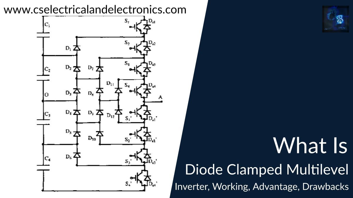
Firstly, in order to generate the multilevel output, we need to divide the dc input voltage into the number of levels using capacitors (the diode here is used as a clamping device to clamp the dc bus voltage so as to achieve steps in the output voltage of the inverter). If the user is expecting m number of levels (i.e., m levels at the output) then (m-1) no of capacitors are required.
For e.g. for a 5-level inverter, we will be requiring (5-1) i.e., 4 capacitors and these four capacitors will divide the voltage into four different ranges. The voltage across each capacitor will be the same and is given by. So, according to our example above we will have different five levels which are 0, Vdc/4, Vdc/2, 3Vdc/4, and Vdc.
Circuit Topology and Principle of Operation
The simplified circuit diagram of a three-level diode-clamped multilevel inverter is shown in the figure below. For three levels we need (m-1) no of capacitors, [2(m-1)] no of switching devices, and [(m-1)(m-2)] no of clamping diodes for each leg. Each inverter leg is composed of four active switches along with four anti-parallel diodes.
To break the input voltage Vd into two parts we have connected two capacitors as Cd1 and Cd2 which provides the neutral point i.e., Z. Then Dz1 and Dz2 are the two clamping diodes that are used to handle the reverse voltage. Multiple voltage levels are obtained at the output using diodes through various phases of capacitor banks which are connected in series. Practically, we need switches that have bi-directional power flow and blocking voltage capability thus, IGBT can be selected as the switching device.

Whenever we turn ON the switches i.e., S2 and S3, the output terminal of the inverter (A) gets connected to the neutral point through any of the clamping diodes. The voltage across both dc capacitors is E which is normally equal to half of the total dc input voltage. With the neutral current iz the capacitors can be charged and discharged (with a finite value of Cd1 and Cd2) which leads to neutral point current deviation.
Now there are certain steps to synthesize the three-level output voltages. In order to understand the circuit in detail we consider one phase and analyze it in detail so that we can also understand the other phases (other phases are identical).

The midpoint of the two capacitors is accessed by the converter.
01. The switching state “a” indicates that the upper two switches of leg A are ON and the terminal voltage given by Vao, which is the voltage at terminal A with respect to neutral point O is Vd/2.
02. Switching state “b” from the figure above illustrates that the two inner switches S2 and S3 conduct and the voltage Vao is clamped to zero using clamping diodes. On the basis of the direction of the load current iA, one of the clamping diodes is turned ON. For example, if there is a positive load (i.e., iA>0) makes the diode D5 turn ON, and terminal A is connected to the neutral point O through the conduction of D5 and S2 and vice-versa.
03. When the two lower switches conduct i.e., switching state “c” which is switch S3 and S4 leads conduction of diodes D3 and D4 which yields a voltage equal to -Vd/2.
The table below shows the voltage levels and their corresponding switching states. When the state condition is 1 it means the switch is ON and when it is 0 it means the switch is OFF.
| Vao | S1 | S2 | S3 | S4 |
| Vdc/2 | 1 | 1 | 0 | 0 |
| 0 | 0 | 1 | 1 | 0 |
| -Vdc/2 | 0 | 0 | 1 | 1 |
In this phase leg, the switches S1 and S3 are complementary, and switches S2 and S4 are complementary (i.e., with one switch ON the other must be OFF).
Applications
The diode clamped has the following field of applications:
- Static VAR Compensations: To maintain the system’s power factor within the desirable range (~ unity) the reactive power is adjusted. The diode-clamped multilevel inverter provides us with a very fast as well as effortless reactive power (VAR) compensation.
- High voltage system interconnections are another application of this inverter.
- This inverter can also be used for interfacing with the DC- AC transmission grid systems.
- The variable speed drives use this inverter as it helps to control and maintain the speed very well and also contributes to conserving energy and improves the life span of the device.
Advantages
- The method of control is simple enough.
- There is no (or small) need for filters as the harmonic content is very low.
- The switching of all devices at fundamental frequencies causes the efficiency to be high.
- All of the phases share a common dc bus that is used by all three phases and thus the requirement of capacitance is reduced and the source can be single.
- It works very efficiently for back-to-back high-power connections.
- Low dv/dt
Disadvantages
- With the increasing no of levels, the no of clamping diodes to be used also increases (as it needs high voltage and different rating diodes to block the reverse voltages) thus, making the circuit configuration more complicated.
- The control of real power flow shows some difficulty due to capacitor imbalance.
- For levels higher than three the charge balance gets disturbed.
- It is difficult to maintain charging and discharging.
- Complicity increases in the PWM switching pattern with the increasing number of levels.
This was about “What Is Diode Clamped Multi-level Inverter“. I hope this article may help you all a lot. Thank you for reading.
Also, read:
- 10 Tips To Maintain Battery For Long Life, Battery Maintainance
- 10 Tips To Save Electricity Bills, Save Money By Saving Electricity
- 100 (AI) Artificial Intelligence Applications In The Automotive Industry
- 100 + Electrical Engineering Projects For Students, Engineers
- 100+ Indian Startups & What They Are Building


