Hello guys, welcome back to my blog. In this article, I will discuss how chips are made or manufactured, how integrated circuits are formed, the chip manufacturing process, raw materials required to design chips, etc.
If you have any doubts related to electrical, electronics, and computer science, then ask questions. You can also catch me on Instagram – Chetan Shidling.
Also, read:
- Top 20 VLSI & Embedded Systems Projects for Mtech Students
- Top 20 Projects On Power Electronics, Power Electronics Projects
- Roadmap For How To Become An IoT Engineer, Internet Of Things
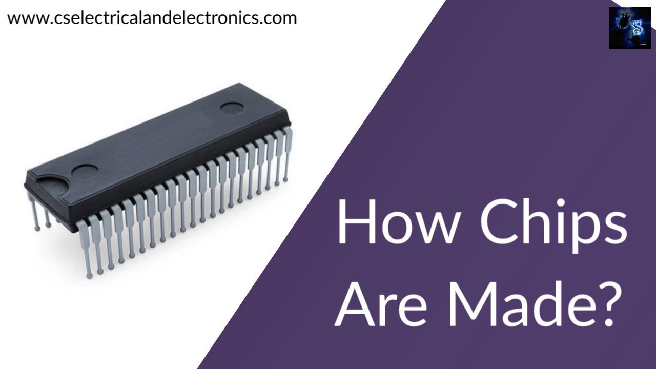
How Chips Are Made Or Manufactured
An integrated circuit, or IC, is a tiny array of electronic circuits and components diffused or implanted onto the surface of a single crystal, or chip, of semiconducting material like silicon. It’s referred to as an integrated circuit.
How Integrated Circuit Are Formed:
Electronic components such as resistors, capacitors, diodes, and transistors are created directly on the surface of a silicon crystal in an integrated circuit. If you first grasp some of the fundamentals of how integrated circuits are made, the manufacturing process will make more sense.
Even before the first integrated circuit (IC) was created, it was recognized that silicon could be used to make ordinary electrical components. How might these, as well as the connecting circuits, be made from the same piece of silicon? The answer was to change the chemical makeup of small regions on the silicon crystal surface, known as dopants, by introducing other molecules.
Some dopants form bonds with silicon, resulting in areas where the dopant atoms can give up one electron. These are referred to as N areas. Other dopants form bonds with the silicon to create areas where the dopant atoms can accept one electron.
These are referred to as P regions. A PN junction occurs when a P area meets an N region on the boundary between them. This 0.000004-inch-wide (0.0001-centimeter-wide) border is critical to the operation of integrated circuit components.
Within a PN junction, the atoms from the two zones bind together to form a third region termed a depletion region, in which the P dopant atoms absorb all of the excess electrons from the N dopant atoms, thereby depleting them.
A positive voltage supplied to the P area can induce an electrical current to pass across the junction into the N region, but a comparable positive voltage applied to the N region will result in little or no current flowing back into the P region.
A PN junction’s capacity to conduct or insulate depending on which side of the voltage is applied may be utilized to create integrated circuit components that direct and regulate current flows in the same way that diodes and transistors do.
A single PN junction, for example, is all that a diode is. Integrated circuit components that mimic the functions of resistors and capacitors may be created by modifying the number and kinds of dopants, as well as the shapes and relative placements of the P and N regions.
Design
Some integrated circuits are called “off-the-shelf” products. There is no need to create anything else after that. Voltage regulators, amplifiers, analog switches, and analog-to-digital or digital-to-analog converters are examples of standard ICs. These ICs are often supplied to other firms for use in printed circuit boards for a variety of electronic devices.
Raw Materials
The majority of integrated circuits are made of pure silicon. Chemically doped to give the N and P regions that make up the integrated circuit components, it serves as the chip’s base or substrate.
Only one out of every 10 billion atoms can be an impurity, therefore silicon must be extremely pure. One grain of sugar in 10 buckets of sand would be equal. Silicon dioxide is utilized in IC capacitors as an insulator and a dielectric material.
Phosphorus and arsenic are two common N-type dopants. P-type dopants include boron and gallium. Connectors between the various IC components are frequently made of aluminum.
Aluminum or gold thin wire leads connect the integrated circuit chip to its mounting package. Ceramic or plastic materials may be used to construct the mounting package.
The Manufacturing Process
Hundreds of integrated circuits are created simultaneously on a single, thin slice of silicon, which is subsequently sliced apart into separate IC chips. The manufacturing process takes place in a clean room, which is a highly regulated environment where the air is filtered to eliminate extraneous particles.
Lint-free clothing, gloves, and head and foot covers are worn by the few machine users in the room. Even the light sources are filtered since some IC components are sensitive to particular light frequencies. The procedure is lengthy and varies according to the type of chip being manufactured. However, the following is a common procedure:
01. A huge, cylindrical piece of silicon crystal being shaved into thin, one-hundredth-inch-thick wafers.
02. Several hundred or thousands of completed integrated circuits will be made from each of these wafers.
03. On top of the wafer, a specific photoresist solution is applied.
04. Over the photoresist, a mask is placed.
05. The mask is a representation of the real circuit, with some sections transparent for light to pass through and others opaque to prevent it.
06. The wafer is subjected to extremely high levels of UV radiation.
07. The wafer is etched under the transparent regions of the mask by ultraviolet radiation, while the areas under the opaque parts of the mask remain unaffected.
08. The mask is removed, and any photoresist residue is wiped away.
09. After that, the wafer is subjected to a doping substance.
10. In the etched portions of the wafer, this results in n-type and p-type regions.
11. The technique is repeated for each layer until all of them are complete.
12. This, of course, presupposes that the circuit design asks for several layers to be layered on top of each other.
13. After that, the individual integrated circuits are disassembled and installed in their final package.
To sum up, It’s difficult to say with any surety what the integrated circuit’s future holds. Since the development of the gadget, technology has evolved at a rapid pace. The architecture, or circuit layout, on a chip, has changed significantly, but the integrated circuit remains a silicon-based design.
This was about how chips are made or manufactured. I hope this article “How Chips Are Made” may help you all a lot. Thank you for reading “How Chips Are Made”.
Also, read:
- 10 Free ADAS Projects With Source Code And Documentation – Learn & Build Today
- 10 Tips To Maintain Battery For Long Life, Battery Maintainance
- 10 Tips To Save Electricity Bills, Save Money By Saving Electricity
- 100 (AI) Artificial Intelligence Applications In The Automotive Industry
- 100 + Electrical Engineering Projects For Students, Engineers
- 100+ Indian Startups & What They Are Building
- 1000+ Automotive Interview Questions With Answers
- 1000+ Electronics Projects For Engineers, Diploma, MTech Students