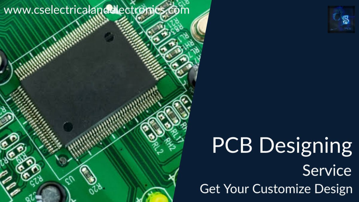
PCB (printed circuit board) design is the process of creating the physical layout for a PCB. This involves determining the size and shape of the board, the placement of the various components, and the routing of the electrical connections between the components.
PCB design can be done manually using pencil and paper, or it can be done using specialized software. The latter approach is more common, as it allows for faster and more accurate design, as well as easier modification and collaboration.
There are several key steps involved in PCB design, including the following:
- Defining the requirements for the PCB, including the size and shape of the board, the number and type of components, and the electrical and mechanical requirements.
- Creating a schematic diagram, which is a high-level representation of the electrical connections between the components. This is typically done using schematic capture software.
- Placing the components on the PCB involves determining the optimal locations for each component based on factors such as space constraints, component tolerances, and electrical requirements.
- Routing the electrical connections between the components, which involves creating the physical pathways that the electrical signals will follow on the PCB. This is typically done using routing software, which can automatically generate the routing based on the components and their connections.
- Validating the design, which involves simulating and testing the PCB to ensure that it meets the requirements and functions as intended. This can include checking for electrical issues such as shorts and opens, as well as mechanical issues such as clearance and spacing.
Once the PCB design is complete, it can be used to create the actual PCB using manufacturing processes such as etching and drilling.
Best tools for PCB designers
There are many tools available for PCB designers, and the best ones will depend on the specific requirements and preferences of the designer. Some of the most common and widely used tools for PCB design include the following:
- Schematic capture software, such as Altium Designer, OrCAD, or KiCad, is used to create the schematic diagram for the PCB.
- PCB layout software, such as Altium Designer, OrCAD, or Eagle, which is used to place the components on the PCB and route the electrical connections.
- Simulation software, such as LTspice or PSpice, is used to simulate the electrical behavior of the PCB and verify that it functions as intended.
- Manufacturing software, such as CAM350 or GerberLogix, is used to generate the manufacturing files that are used to create the actual PCB.
- CAD software, such as AutoCAD or SolidWorks, which is used to create 3D models and renderings of the PCB for visualization and presentation.
In addition to these tools, PCB designers may also use a variety of other tools and equipment, such as oscilloscopes, multimeters, and 3D printers, to aid in the design and validation of their PCBs.
Need Support?
[fluentform id=”7″]