Hello guys, welcome back to our blog. This article will be on what is SPI protocol, a serial peripheral interface, an SPI tutorial for beginners, working of SPI (we will cover in detail SPI modes, how to configure SPI), advantages, disadvantages, and applications of SPI.
If you have any electrical, electronics, and computer science doubts, then ask questions. You can also catch me on Instagram – CS Electrical & Electronics.
Also, read:
- Difference Between Sine, Square, And Modified Sine Wave Inverters
- What Is Emulator, Debugger, Assembler, Compiler In Embedded Tools
- What is PyroSwitch In Electric Vehicle, Working, Purpose, Advantages
What Is SPI Protocol
If you attach a microcontroller to a sensor, different input, display, or another module, do you ever assume how the two devices chat together? What precisely are they saying? How are they capable to understand together?
Contact between electronic apparatuses is like contact between humans. Both sides require to speak the exact language. In electronics, these languages are named communication protocols.
Introduction to SPI / Serial Peripheral Interface
SPI (Serial Peripheral Interface) is an interface bus typically utilized for communication with sensors, flash memory, analog-to-digital converters, real-time clocks (RTCs), and more. The Serial Peripheral Interface (SPI) bus was designed by Motorola to deliver full-duplex synchronous serial communication between slave and master apparatuses.
Serial Peripheral Interface is a data transmission protocol that we utilize for controlling devices within a subsystem, especially sensors.
SPI is a communication protocol utilized to talk or communicate between microcontrollers and peripheral apparatuses, such as displays, and sensors. In simple words, it’s a system that permits us to transmit a byte to some device and accept a byte in return.
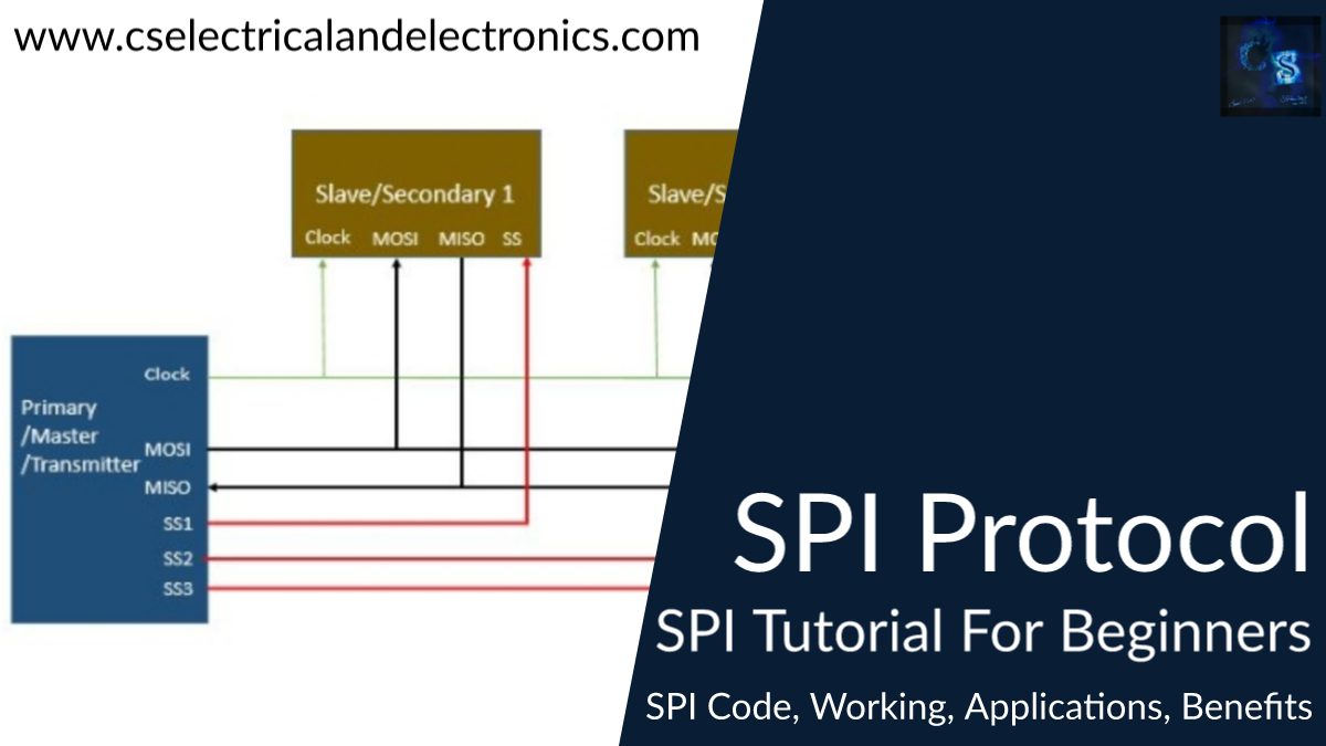
SPI utilizes amazing architecture, called a Master-Slave architecture. In this method, there is one master apparatus or device that communicates to numerous slave devices. In our approach, the master device is our microcontroller and the slave devices are especially extension displays or sensors. The master can only convey with one slave device at a time and the slaves cannot talk or communicate with each other.
SPI or Serial Peripheral Interface is a synchronous serial communication protocol that delivers full-duplex communication at extremely high speeds. Serial Peripheral Interface (SPI) is a master-slave kind protocol that provides a straightforward and low-cost interface between sensors, microcontrollers, and peripherals.
SPI Interface bus is generally utilized for interfacing microcontroller or microprocessor with a memory like RTC (Real Time Clock), EEPROM, DAC (Digital – to – Analog Converters), ADC (Analog – to – Digital Converters), displays like LCDs, Audio ICs, memory cards like MMC or SD Cards, sensors like temperature and pressure, or even other microcontrollers.
I2C, SPI, and UART are slower than protocols like Bluetooth, USB, ethernet, and WiFi, but they’re easier and utilize less hardware and design resources. I2C, SPI, and UART are perfect for contact or communication between microcontrollers and sensors where enormous amounts of high-speed data don’t require to be transmitted.
Difference between serial and parallel communication
Electronic apparatuses communicate or talk to each other by transmitting bits of data via wires physically attached between devices. For example, a bit is like a letter in a word, besides instead of the 26 letters (in the English alphabet), a bit is binary and can just be a 1 or 0. Bits are transmitted from one apparatus to another by rapid transformations in voltage. In a design operating at 5 V, a 0 bit is transmitted as a short pulse of 0 V, and a 1 bit is transmitted by a short pulse of 5 V.
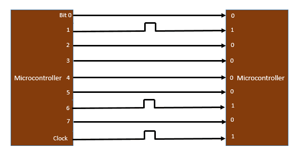
The bits of data can be sent either in serial or parallel form. In parallel transmission, the bits of data are transmitted all at the same time, each via a separate wire. The subsequent diagram shows the parallel communication of the letter “B” in binary (01000010):
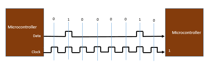
In serial transmission or communication, the bits are transmitted one by one via a single wire. The next diagram shows the serial communication of the letter “B” in binary (01000010):
Working of SPI / Serial Peripheral Interface
SPI is a Synchronous kind of serial communication i.e. it employs a reliable clock signal to synchronize the primary and secondary or Master and Slave or transmitter and receiver, communicating in SPI terms. The primary and secondary are connected with different data and clock lines and the clock signal will allow the secondary when to look for data on the bus.
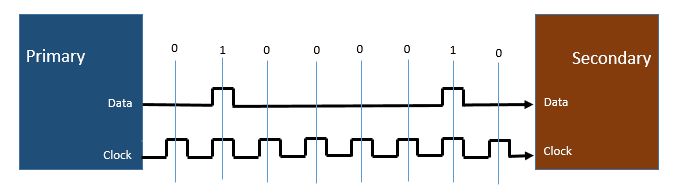
The clock signal must be provided by the Primary to the Secondary (or all the Secondaries in case of multiple secondaries setups). There are two kinds of triggering techniques on the clock signal that are utilized to contact the secondary about the data: Level Triggering and Edge Triggering.
The most generally utilized triggering is edge triggering and there are two kinds: falling edge (high to low transition) and rising edge (low to high transition on the clock). Relying on how the secondary is configured, upon witnessing the edge, the secondary will examine for data on the data bus from the following bit.
Since both the data and clock are transmitted by the Primary (or transmitter), we need not bother regarding the speed of data transfer.
What drives SPI so famous among other serial communication is that it delivers high-speed secured data transfer with politely uncomplicated hardware like shift registers at somewhat less cost.
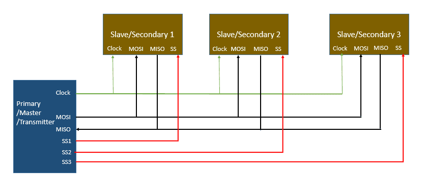
In Serial Peripheral Interface protocol, there can be only one primary but many secondary devices.
The Serial Peripheral Interface bus contains 4 pins or signals. They are
- MOSI or Master – Out / Slave – In
- MISO or Master – In / Slave – Out
- SCLK or Serial Clock and
- Slave Select (SS) or Chip Select (CS)
In digital approaches, data is transmitted in the state of 1’s and 0’s. In hardware, 1’s and 0’s are described as high and low voltages. Our system employs 5 volts, so a 1 corresponds to ~5 volts on a wire, and a 0 corresponds to ~0 volts.
SPI is a synchronous communication protocol, indicating data is timed with clock pulsations. is transmitted and accepted in the same period. This suggests that two of the 4 lines (MISO, MOSI) are for data, and one of the lines (Clock) is for timing.
SPI employs 4 wires to transmit, which are directed to the SPI bus. Three lines (clock, MOSI, MISO) are conveyed between all apparatuses on an SPI bus. The 4th line (CS/SS) is special to every secondary or receiver device, and all CS/SS lines are connected to the primary device.
The primary device constantly sends a square wave on the clock to synchronize all machines. To start transmission, the primary device sets chip select/slave select (SS) low for a precise device. The primary device transmits data to the secondary device on the MOSI or master(primary) out, slave(secondary) line. During the same period, the secondary device transmits data to the primary device on the MISO or master in, slave(secondary) out line. To stop transmission, the primary device sets CS/SS high again.
Well guys, let me quick recall things. The primary device outputs the clock signal. The primary controls the SS/CS pin to a lower voltage state (0), which starts the secondary. The primary transmits the data one bit at a period to the secondary along the MOSI line. The secondary reads the bits as they are received from the primary. If a reply is needed, the secondary returns data one bit at a period to the primary along the MISO line. The primary read the bits as they are obtained.
01. Clock: The clock controls the data lines and devices in sync. The clock is an oscillating signal delivered by the primary device that suggests to the secondary or receiving device when to read the data. Relying on the device’s possessions, data is either sent/received on the falling or rising edge of the clock. This line is shared by all secondary devices.
02. MOSI or master out, slave(secondary) in: This is the stripe where data is transmitted from the primary device to the secondary device. This line is communicated by all secondary devices.
MISO pins on to sides of the primary and secondary are jointly together. Even though the Signal in MISO is produced by the secondary, the line is controlled by the Primary. The primary (master) induces a clock signal at clock or SCLK and is provided to the clock input of the secondary or slave. Chip Select (CS) or SS or Slave Select is utilized to specify a particular secondary by the master or primary.
Since the clock is induced by the Primary or Master, the flow of data is handled by the primary or master. For each clock cycle, one bit of data is transferred from primary to secondary and one bit of data is transferred from secondary to primary (master).
This thing occurs simultaneously and behind 8 clock cycles, a byte of data is transferred in both paths therefore, SPI is a full-duplex transmission. If the data has to be transferred by only one device, then the other apparatus has to send something (even junk data or garbage) and it is up to the device whether the transferred data is real data or not.
This suggests that for every bit transferred by one device, the other apparatus has to transmit one-bit data i.e. the Primary simultaneously sends data on the MOSI line and accepts data from the secondary on the MISO line. If the secondary desires to transfer the data, the primary has to generate the clock signal therefore by understanding when the secondary desires to transmit the data in advance. If more than one slave or secondary has to be connected to the primary or master, then the setup will be something equivalent to the above image with a number of secondaries.
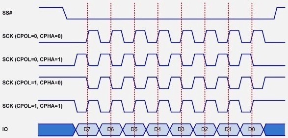
SPI Modes: Clock Polarity & Phase Polarity
Clock polarity or CPOL and clock phase or CPHA can be defined as ‘0’ or ‘1’ to create four special methods to deliver flexibility in contact between primary or master and secondary or slave as shown in the below figure.
Even though numerous secondaries or slaves are attached to the primary or master in the SPI bus, only one secondary or slave will be active at any moment. In demand to select the secondary or slave, the primary or master will pull down the CS (Chip Select) or SS (Slave Select) line of the corresponding slave.
Therefore, there must be a different CS pin on the Primary or Master corresponding to each of the secondary or slave devices. We must pull down the SS bar to set the secondary or slave because this line is active (0) low.
We have already witnessed that it is the assignment of the Primary or Master device to induce the clock signal and spread it to the secondary or slave in charge to synchronize the data between primary and secondary. The outcome of the master doesn’t end with developing clock signals at a special frequency.
In point, the primary and secondary have to decide on specific synchronization protocols. For this, two components of the clock i.e. the Clock Phase (CPHA) and Clock Polarity (CPOL or CKP) come in to picture.
Clock Polarity specifies the state of the clock. When CPOL is LOW, the clock induced by the Primary or Master i.e. SCK is LOW when inactive and toggles to HIGH during the active form (during a transfer). Again, when CPOL is HIGH, SCK or clock is HIGH during inactive and LOW during the active state.
Clock Phase specifies the clock change. i.e., falling (HIGH to LOW) or rising (LOW to HIGH), at which the data is transferred. When CPHA is 0, the data is transferred on the rising edge of the clock. Data is transferred on the falling edge when CPHA is 1.
Relying on the values of Clock Phase (CPHA) and Clock Polarity (CPOL), there are 4 modes of the process of SPI: Modes 0 through 3.
- If CPOL and CPHA both are ‘0’ (taken as Mode 0) data is tested at the highest rising edge of the clock. Mode 0 is by far the numerous standard mode for SPI bus slave transmission.
- If CPOL is ‘1’ and CPHA is ‘0’ (taken as Mode 2), data is tested at the maximum falling edge of the clock.
- Also, if CPOL = ‘0’ and CPHA = ‘1’ (taken as Mode 1) results in data tested on the trailing falling edge, and
- if CPOL = ‘1’ with CPHA = ‘1’ (taken as Mode 3) results in data tested on the trailing rising edge.
SPI Embedded C Code
The code utilizes the common nomenclature for the SPI strings. The MAXQ2000 processor is the SPI primary or master and the MAX7456 is the SPI secondary or slave.
- CS is identical as is utilized in the MAX7456 data sheet.
- SDIN is directed to as MOSI (master out slave in).
- SDOUT is directed as MOSI (master in slave out).
- SCLK is directed to as CK.
The prefix SPI_ is utilized on all lines.
/* This is utilized to access the pins for the SPI port separately. */
/* Port 5 Output Register */

__no_init volatile __io union
{
  unsigned char PO5;
  struct
  {
    unsigned char bit0          : 1;
    unsigned char bit1          : 1;
    unsigned char bit2          : 1;
    unsigned char bit3          : 1;
    unsigned char bit4          : 1;
    unsigned char bit5          : 1;
    unsigned char bit6          : 1;
    unsigned char bit7          : 1;
  } PO5_bit;
}
This code allocates a single byte to PO5, which is the address of the controller’s output port. It then allocates another byte to the exact memory address that can be accessed bit by bit. Thus, the port can be addressed instantly by utilizing commands like PO5 = 0x10;
Or bit by bit by utilizing commands like PO5_bit.bit4 = 1;
Macros
#define SPI_CS         PO5_bit.bit4             // PO5_bit.bit4 = active-low CS—chip select
#define SPI_MOSI       PO5_bit.bit5          // PO5_bit.bit5 = MOSI—master out slave in,
                                                                      // data to MAX7456
#define SPI_MISO       PI5_bit.bit7            // PO5_bit.bit7 = MISO—master in slave out,
                                                                      // data from MAX7456
#define SPI_CK         PO5_bit.bit6            // PO5_bit.bit6 = SCK - SPI clock
Code for a single-byte write operation
void spiWriteReg(const unsigned char regAddr, const unsigned char regData)
{

  unsigned char SPICount;                 // Counter used to clock out the data

  unsigned char SPIData;                   // Define a data structure for the SPI data

  SPI_CS = 1;                                         // Make sure we start with active-low CS high
  SPI_CK = 0;                                        // and CK low

  SPIData = regAddr;            // Preload the data to be sent with Address
  SPI_CS = 0;                          // Set active-low CS low to start the SPI cycle
                                               // Although SPIData could be implemented as an "int",
                                               // resulting in one
                                               // loop, the routines run faster when two loops
                                               // are implemented with
                                              // SPIData implemented as two "char"s.

  for (SPICount = 0; SPICount < 8; SPICount++)                  // Prepare to clock out the Address byte
  {
    if (SPIData & 0x80)               // Check for a 1
      SPI_MOSI = 1;                      // and set the MOSI line appropriately
    else
      SPI_MOSI = 0;
    SPI_CK = 1;                             // Toggle the clock line
    SPI_CK = 0;
    SPIData <<= 1;                      // Rotate to get the next bit
  }                                                // and loop back to send the next bit

                                                   // Repeat for the Data byte
  SPIData = regData;                // Preload the data to be sent with Data
  for (SPICount = 0; SPICount < 8; SPICount++)
  {
    if (SPIData & 0x80)
      SPI_MOSI = 1;
    else
      SPI_MOSI = 0;
    SPI_CK = 1;
    SPI_CK = 0;
    SPIData <<= 1;
  }
  SPI_CS = 1;
  SPI_MOSI = 0;
}
Advantages of SPI Protocol
- SPI is extremely easy to execute and the hardware needs are not that complex.
- Keeps full-duplex communication at all times.
- Extremely high speed of data transfer.
- No beginning and stop bits, so the data can be streamed continually without interruption
- No complex secondary or slave addressing system like I2C
- More increased data transfer rate than I2C (almost twice as fast)
- Different MISO and MOSI bars, so data can be transmitted and received at the exact time
- No requirement for unique addresses for slaves as CS or SS is employed.
- Only one primary or master device is kept and hence there is no possibility of conflicts.
- The clock from the primary or master is configured based on the speed of the slave and therefore secondary or slave doesn’t have to stress about the clock.
Disadvantages of SPI Protocol
- Utilizes four wires (I2C and UARTs utilize two)
- There is no declaration mechanism and therefore there is no guarantee of receipt of data.
- Each other secondary or slave needs an additional reliable pin on the primary or master for CS or SS.
- No form of error scanning like the parity bit in UART
- Only qualifies for a single master
- The slowest device specifies the speed of transfer.
- There are no authorized standards and hence often utilized in application-specific implementations.
- There is no flow management.
Applications Of SPI Protocol
- For communicating between parameter measurement sensor and microcontrollers
- Memory: EEPROM, Flash, SD Card, MMC
- Sensors: Temperature and Pressure
- Control Devices: digital POTS, ADC, DAC, and Audio Codec.
- Others: LCD, RTC, video game controller, Camera Lens Mount, touchscreen, etc.
This was about “What Is SPI Protocol“. I hope this article may help you all a lot. Thank you for reading.
Also, read:
- 10 Free ADAS Projects With Source Code And Documentation – Learn & Build Today
- 100 + Electrical Engineering Projects For Students, Engineers
- 100+ Indian Startups & What They Are Building
- 1000+ Automotive Interview Questions With Answers
- 1000+ Electronics Projects For Engineers, Diploma, MTech Students
- 1000+ MATLAB Simulink Projects For MTech, Engineering Students
- 2000+ Embedded Systems Interview Question Bank
- 2026 Hackathons That Can Change Your Tech Career Forever